A Four Billion Dollar Groundbreaking, Four Years From Its First Chip
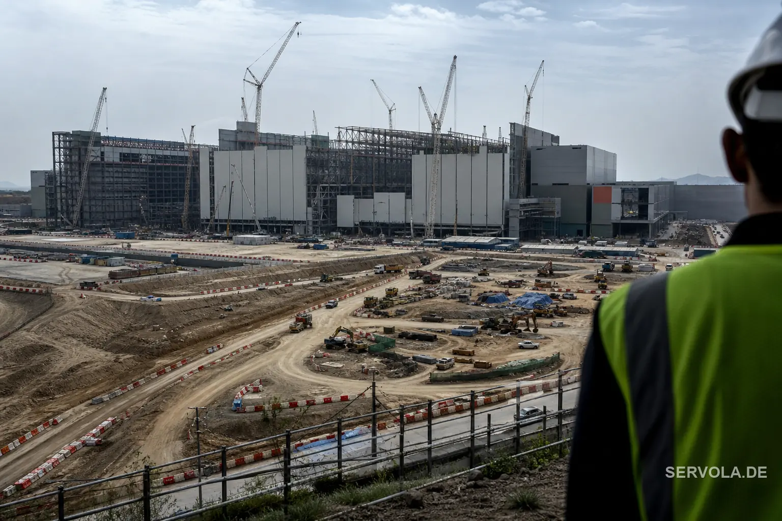
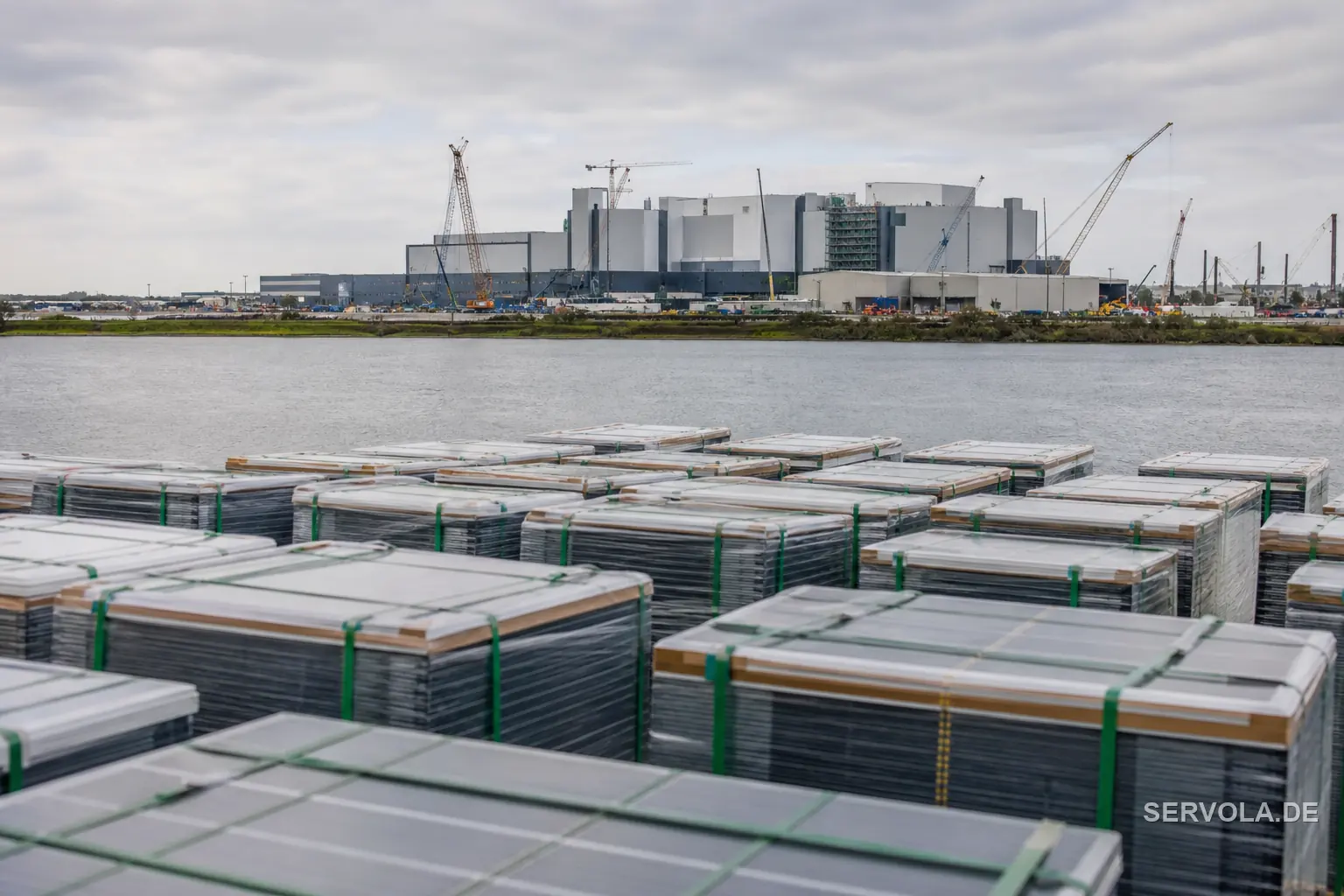
SK Hynix broke ground on August 27, 2026 on a new HBM packaging and test plant at Purdue Research Park in West Lafayette, Indiana, and the company was explicit that the site will not ship a finished chip before the second half of 2029.
The project carries more than $4 billion in capital spending. The cleanroom is targeted for completion in October 2028, with mass production of next-generation HBM to follow roughly a year later. SK Hynix is receiving up to $458 million in direct CHIPS Act grants and has been offered a further $500 million in federal loans toward the cost.
At full operation the site is expected to employ around 1,000 people directly. SK Hynix cites roughly 7,000 direct and indirect jobs once construction, operations, and partner-company activity are counted together, and the company has signed a memorandum of understanding with Purdue University for joint research into advanced packaging and system integration.
The Wafers Still Come From Korea
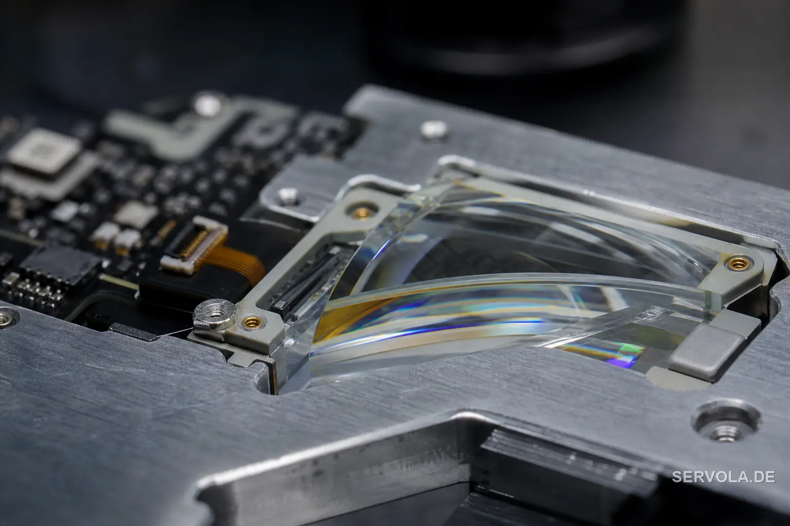
The headline framing, an American HBM plant, undersells what is actually moving across the Pacific. High-bandwidth memory is built in two distinct stages: a base memory wafer is fabricated first, and separately, several of those wafers are stacked using through-silicon vias and packaged into the finished module before final test. Indiana is being built for the second stage only.
SK Hynix says plainly that advanced wafers produced in South Korea will be shipped to Indiana for packaging and testing, after which the finished product is supplied as a Made-in-USA HBM component. Wafer fabrication itself, the most capital-intensive and technically demanding step, stays exactly where it has always been.
That distinction is not a technicality. A packaging plant can be replicated in a new country in a few years once the process is proven; a leading-edge memory fab cannot, which is why SK Hynix, Samsung, and Micron have kept the overwhelming majority of their wafer capacity concentrated in South Korea, Japan, and a handful of long-established US sites.
What This Changes, and What It Does Not, for AI Buyers
For a European or UK operator buying AI accelerators, GPUs, or cloud capacity built on HBM, the practical upside of the Indiana plant is a shorter, more diversified last-mile step: packaging and test capacity that no longer sits entirely in Asia, and a small hedge against disruption at that one stage.
What it does not do is address the constraint that has kept HBM prices elevated through 2026: wafer fabrication capacity, which remains concentrated in South Korea and subject to the same export-control, geopolitical, and natural-disaster risks it always faced. A disruption to SK Hynix's Korean fabs would still halt the pipeline long before it reaches Indiana.
Buyers who treat a Made-in-USA HBM plant as proof the supply chain has been de-risked are reading past what SK Hynix itself describes: a packaging and test site integrated with, not independent of, its South Korean operations. The practical response for anyone budgeting AI infrastructure through 2029 is the same one that applied before the groundbreaking: keep supplier diversification and buffer-stock assumptions tied to wafer capacity, not to where the finished chip gets its final label.
Read next: Mistral Raised 3 Billion, Samsung Got a Chip Model | The 518 Billion Dollar Memory Fix Lands in 2028