What Sony and TSMC actually confirmed on 10 August
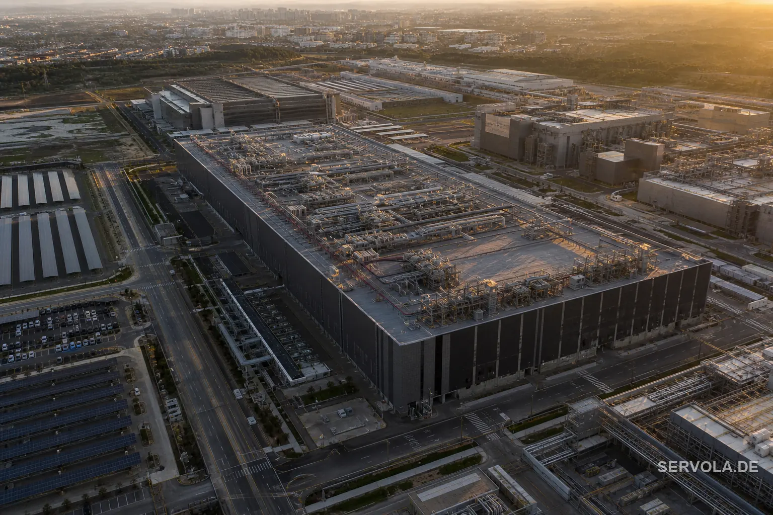
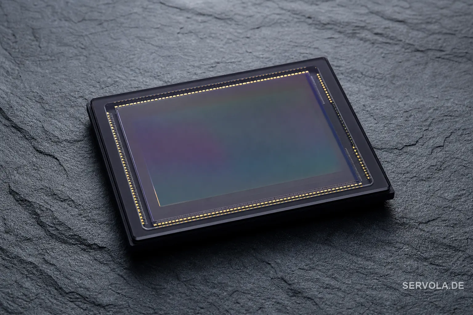
Nikkei Asia reported on 10 August that Sony and TSMC have agreed to invest roughly 1 trillion yen, about 6.3 billion dollars, in a joint venture to build an advanced image sensor plant in Kumamoto, in southern Japan. Sony will hold approximately 60 percent of the venture and TSMC approximately 40 percent. Commercial production is targeted to start as early as 2029. Reuters wire coverage corroborated the figures and reported that the companies are explicitly framing the plant around demand from artificial intelligence, robotics and automotive sensor applications rather than smartphones alone, which is where Sony's sensor business has historically concentrated.
None of this is a cold start. Sony Semiconductor Solutions and TSMC signed a non-binding memorandum of understanding on 8 May 2026 to form the same joint venture, with development and production lines planned for a new fab in Koshi City, Kumamoto Prefecture, alongside new capital investment at Sony's existing Nagasaki plant. Sony chief executive Shinji Sashida called the venture, in the companies' own announcement, a move that brings together the strengths of both companies, and TSMC senior vice president Kevin Zhang described it as underscoring their shared commitment to leading sensing technology. What 10 August adds is the number, the split and the date: preliminary intent has become a priced, timed commitment. Sony declined to comment on the Nikkei report and TSMC did not immediately respond to Reuters, which is standard practice around figures still awaiting a definitive agreement, not a denial of the substance.
The plant that went dark thirteen days earlier
On 28 July 2026, at around 4:27pm local time, a magnitude 7.1 earthquake struck the Kumamoto region. Sony Semiconductor Manufacturing Corporation halted operations at its Kumamoto Technology Center in Kikuyo-machi, the site responsible for the core of Sony's image sensor output. Independent reporting puts that single site's share of global image sensor shipments at roughly 40 to 43 percent, covering sensors used in smartphones, digital cameras and automotive driver-assistance systems. Sony confirmed no casualties among staff and reported no significant damage at its three other regional sites in Nagasaki, Oita and Kagoshima. The Kikuyo plant was not so fortunate: building and manufacturing-line damage required a full safety inspection before any line could restart.
TSMC was not a bystander. Its Japan Advanced Semiconductor Manufacturing fab, known as JASM, sits in the same town of Kikuyo and makes the logic chips that pair with Sony's sensors; TrendForce reported on 3 August that JASM's Fab 1 was placed under inspection after the quake alongside Sony's own restart. Sony began a phased resumption of Kumamoto Technology Center operations on 4 August and targeted a return to pre-quake output by mid-August. That recovery was still in progress, by Sony's own published timeline, when the 1 trillion yen investment was confirmed on 10 August. The joint venture was priced and dated while the region's existing plants were still catching up from the last one.
Kumamoto has done this before
This is not a first occurrence. A magnitude 7.0 earthquake struck the same prefecture in April 2016 and knocked Sony's and Fujifilm's sensor lines offline for weeks. Camera and lens shipments were backordered worldwide well into that autumn, and Sony needed months to fully restore output at the Kumamoto complex. Sony's global CMOS image sensor share was already around 40 percent at the time, which is why a regional earthquake became an industry-wide supply story rather than a local one. The 2026 quake repeated the pattern almost exactly, down to the affected town.
The reason the two companies cluster here anyway is on the record. TSMC's JASM venture exists in the first place because Sony's own chip orders already accounted for more than half of TSMC's sales in Japan, and Sony asked TSMC for a dedicated facility rather than compete for capacity elsewhere. That is a rational answer to a supplier's own volume problem. It says nothing about whether concentrating the next generation of sensor manufacturing in the same seismic corridor is the right answer for the companies that buy from Sony and TSMC downstream, which is a different question with a different set of interests.
Why they are doubling down instead of diversifying
The new joint-venture fab in Koshi City sits in the same prefecture as, and a short distance from, both the Sony plant and the TSMC fab that the July earthquake had just forced offline. Sony and TSMC's logic for staying is straightforward: a trained workforce, an established supplier network and Japanese government incentives are already in place in Kumamoto, and building a comparable cluster from nothing elsewhere would cost years, not months. Speed to the 2029 production target argues for building next to what already exists, not away from it.
That is a rational calculation for Sony and TSMC. It is not automatically the right calculation for their customers. A supplier optimizing for time-to-volume and cost is not optimizing for a buyer's continuity of supply, and the two goals happened to point in opposite directions twice in three weeks this summer: an earthquake shut two Kumamoto plants down on 28 July, and a third major facility for the same product category was priced into the same prefecture on 10 August. Buyers who assumed diversification would follow a disruption of that scale got the opposite result.
What this means for a 2029 vision hardware roadmap
For an EU or UK automotive OEM, Tier 1 supplier, robotics integrator or industrial vision company, the practical fact is simple: production from this joint venture starts as early as 2029, which means components being specified today for model-year 2029 and 2030 vehicle platforms, or for the next generation of warehouse and factory robots, will draw on sensor silicon made in this cluster. That is not a distant, hypothetical dependency. It is a design decision being made now, on a bill of materials being locked now, against a supply base that has twice gone dark for weeks inside the last decade.
The useful response is not to avoid Sony or TSMC, which between them supply a large share of the sensors and logic chips the industry runs on and have no full performance-parity substitute at scale. It is to name the exposure on paper. Ask any vendor whose components trace back to Kumamoto for a written second-source qualification path or a documented buffer-stock policy covering earthquake-class disruption, and build that lead-time cushion into 2028 and 2029 launch schedules before the spec locks, not after the next plant goes offline.
Read next: The Chip Fix Everyone Is Celebrating Ships In 2033 | Xbox Picked Up the Risk Sony Walked Away From