Three New Names Built on One Bonding Technique
At the Future of Memory and Storage (FMS) 2026 conference in Santa Clara, Samsung DRAM Design Team vice president Kyungryun Kim and Flash Product and Technology executive vice president Jin-Yub Lee presented three new memory architectures, all built on advanced wafer-bonding technology. zHBM stacks high-bandwidth memory directly on top of an AI accelerator chip instead of placing it beside the processor, and Samsung's own projections put a next-generation interface system using zHBM at roughly 8x the performance of HBM5, more than 10x the memory density, a threefold gain in energy efficiency, and better than a 50 percent cut in thermal resistance.
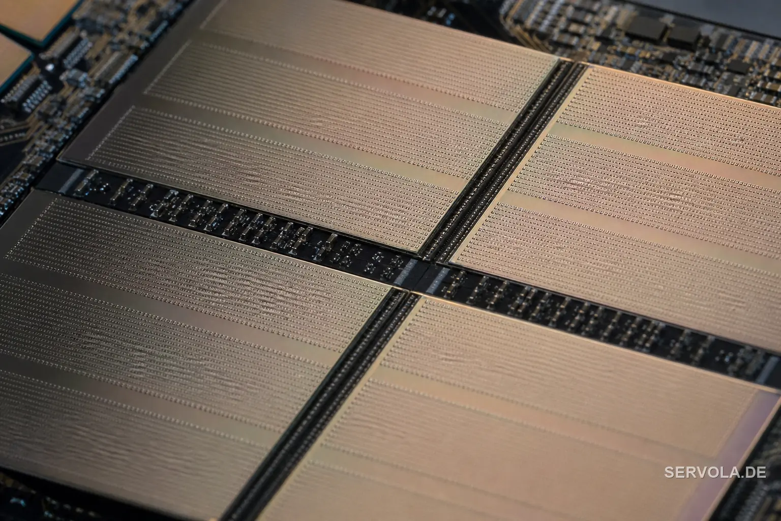
zNAND-O is a high-performance NAND design built on Samsung's V-NAND line, offered in four- and eight-layer versions and aimed at edge AI workloads that need low latency and real-time processing. V10 BV-NAND is the concrete product of the three: more than 400 layers, built with wafer bonding rather than a conventional single-stack etch, and about 58 percent denser than Samsung's prior V9 generation, with better read, write, and I/O performance.
A Vision Model and a Shipping Chip Are Different Claims
Samsung itself showed zHBM and zNAND-O as concept models, presented alongside products it already ships: HBM4E samples, an HBM5 preview, LPDDR5X-PIM, and the enterprise drives PM1763 and BM1773. Independent industry analysis from Futurum Group sharpens the distinction: V10 BV-NAND is best read as productization of a bonded-NAND concept that rivals including Kioxia, SanDisk, and YMTC have also pursued, with the real competitive edge sitting in bonding-interface yield and alignment precision, not the layer count alone.
Futurum analyst Brendan Burke names three unresolved production hurdles before any of this ships at scale: hybrid-bonding pitch scaling below 10 microns at full DRAM-stack yield, known-good-die testing before an irreversible bond, and thermal extraction, pushing roughly 1 kilowatt of heat through a stacked memory die without degrading data retention. Burke calls the thermal problem the tallest of the three, and it is a materials-science constraint that does not move faster because a roadmap says it should.
The Supply Picture This Does Not Change in 2026
None of this alters the memory market buyers are paying into this year. Samsung already holds about 34.0 percent of data center memory revenue, ahead of SK Hynix at 29.8 percent and Micron at 17.9 percent as of the fourth quarter of 2025, and HBM alone is projected to absorb around a quarter of total DRAM wafer output in 2026.
Analysts tracking the category put the data center off-chip memory market at roughly $17.1 billion in 2025, growing toward $96.8 billion in 2026 and an estimated $260.5 billion by 2030. That is the backdrop an AI buildout has been operating inside through 2025 and 2026: a memory-supply-constrained market tight enough to shape which cloud and chip vendors can promise delivery dates at all, and a concept-model unveiling at a trade show adds no wafer to that supply this year.
What This Means for a European or UK Infrastructure Budget
For an EU or UK enterprise buyer negotiating GPU capacity, a server refresh, or a multi-year cloud contract in 2026, the practical read runs against what a roadmap slide implies. This is not a sign that memory costs are about to ease; it is a supply-side data point showing the vendor with the largest share of data center memory revenue is still years from shipping the technology it says will relieve the bottleneck.
That makes the current shortage the planning baseline for the next one to two budget cycles. The sensible move is to lock in supply and pricing commitments now, while the constraint is known and priced, rather than delaying a contract on the assumption that zHBM-class density gains will show up inside this year's or next year's server refresh.
Reading the Next Year of Memory Announcements
The pattern worth tracking going forward is qualification dates and named customer deployments, not spec-sheet multiples. HBM4E's shipping samples and V10 BV-NAND's stated 400-plus layers are claims with a manufacturing process behind them today; the 8x and 10x figures attached to zHBM describe a target for a system that does not yet exist as a shipping part.
Treat every future memory update the same way: separate what a company is delivering this quarter from what a vision model promises for a generation still working through pitch scaling, die testing, and thermal limits that no press release can shortcut.
Read next: A 30 Billion Dollar Data Center Meets a 5 Billion Dollar Insurance Ceiling | Your Electricity Bill Just Got a Legal Shield From AI Data Centers